Scanning electron microscope (SEM) and microanalysisadmin2021-12-21T13:58:34+00:00
Scanning Electron Microscope (SEM) and microanalysis
The study of the microstructure of the materials is of basic importance to achieve information about:
- compactness (for products not sintered) and sintering degrees, with assessment of the level and type of porosity (closed porosity, open porosity, pore morphology, pore interconnectivity, etc.)
- morphology and composition of powder particles
- morphology and composition of the different phases – crystalline and not – inside a materia
- surface morphology.
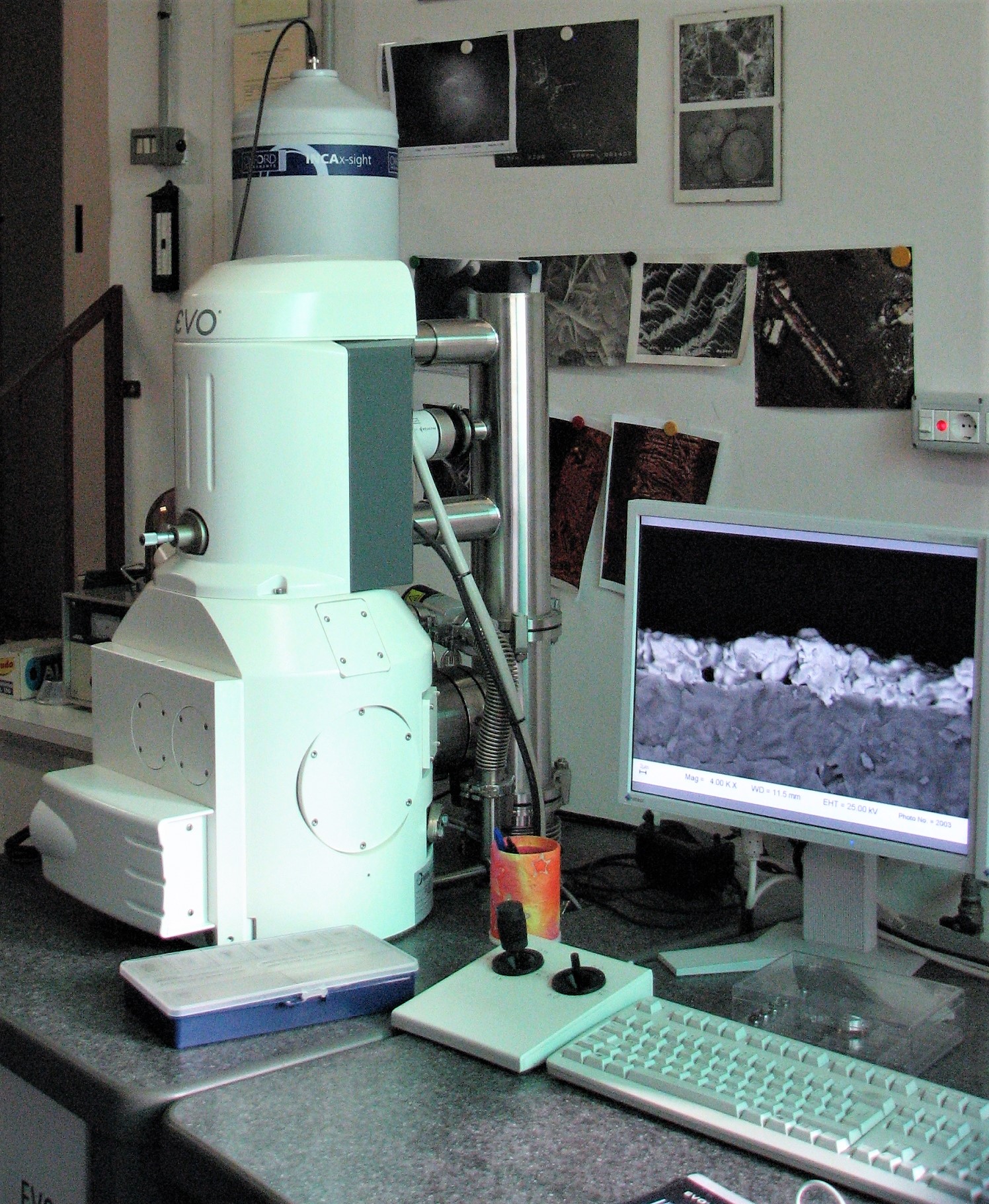
Technical features of the instrument
The laboratory makes use of a Scanning Electron Microscope (SEM) mod. LEO “EVO 40XVP-M”, Zeiss (D), connected to a microanalysis system mod. INCA Energy 250 – Oxford Instruments Analytical Ltd (UK).
The more significant features of the device are:
- High Vacuum and eXtended Variable Pressure (XVP) imaging modes in the range 1-750 MPa, for the analysis of non conducting specimens
- detector of secondary electrons in high vacuum (ET-SE), and detector of backscattered electrons (4QBSE)
- resolution of 3 nm and magnification 7x – 1,000,000x
- qualitative and quantitative elemental analysis software, with standard
- software for mapping chemical elements and for concentration profiles.
Contact person:
Eng. Barbara Mazzanti – e-mail mazzanti@centroceramico.it
Mobile: +39 340 9631182
Services to industry
- microstructure analysis of the materials, both massive and thin film
- analysis of components surface
- fractographic analysis of components.